


| Story Views | |
| Now: | |
| Last Hour: | |
| Last 24 Hours: | |
| Total: | |
IBM Researchers Demonstrate Initial Steps toward Commercial Fabrication of Carbon Nanotube Chip

From
Novel processing method helped pave the way for carbon technology as a viable alternative to silicon in future computing.
IBM scientists have demonstrated a new approach to carbon nanotechnology that opens up the path for commercial fabrication of dramatically smaller, faster and more powerful computer chips. For the first time, more than ten thousand working transistors made of nano-sized tubes of carbon have been precisely placed and tested in a single chip using standard semiconductor processes. These carbon devices are poised to replace and outperform silicon technology allowing further miniaturization of computing components and leading the way for future microelectronics.
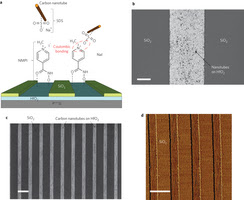
Selective placement of carbon nanotubes by an ion-exchange process.
Nature Nanotechnology – High-density integration of carbon nanotubes via chemical self-assembly
ABSTRACT – Carbon nanotubes have potential in the development of high-speed and power-efficient logic applications. However, for such technologies to be viable, a high density of semiconducting nanotubes must be placed at precise locations on a substrate. Here, we show that ion-exchange chemistry can be used to fabricate arrays of individually positioned carbon nanotubes with a density as high as 1 × 10^9 cm−2—two orders of magnitude higher than previous reports. With this approach, we assembled a high density of carbon-nanotube transistors in a conventional semiconductor fabrication line and then electrically tested more than 10,000 devices in a single chip. The ability to characterize such large distributions of nanotube devices is crucial for analysing transistor performance, yield and semiconducting nanotube purity.


See more and subscribe to NextBigFuture at 2012-10-28 23:03:38 Source: http://nextbigfuture.com/2012/10/ibm-researchers-demonstrate-initial.html
Source:
