


| Story Views | |
| Now: | |
| Last Hour: | |
| Last 24 Hours: | |
| Total: | |
Nanometer-scale diamond tips improve nano-manufacturing

From
One of the most promising innovations of nanotechnology has been the ability to perform rapid nanofabrication using nanometer-scale tips. The fabrication speed can be dramatically increased by using heat. High speed and high temperature have been known to degrade the tip… until now.
“Thermal processing is widely used in manufacturing,” according to William King, the College of Engineering Bliss Professor at Illinois. “We have been working to shrink thermal processing to the nanometer scale, where we can use a nanometer-scale heat source to add or remove material, or induce a physical or chemical reaction.”
One of the key challenges has been the reliability of the nanometer-scale tips, especially with performing nano-writing on hard, semiconductor surfaces. Now, researchers at the University of Illinois, University of Pennsylvania, and Advanced Diamond Technologies Inc., have created a new type of nano-tip for thermal processing, which is made entirely out of diamond.
“The end of the diamond tip is 10 nm in size,” King explained. “Not only can the tip be used for nanometer-scale thermal processing, but it is extremely resistant to wear.”
The research findings are reported in the article, “Ultrananocrystalline diamond tip integrated onto a heated atomic force microscope (AFM) cantilever,” that appears in in the journal Nanotechnology. The study shows how the 10 nm diamond tip scans in contact with a surface for a distance of more than 1.2 meters, and experiences essentially no wear over that distance.
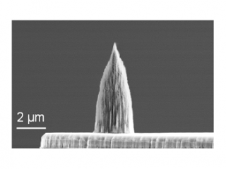
Diamond nano-tip integrated onto the micro-heater of a doped silicon microcantilever. The tip has a radius of 10 nm.
Ultrananocrystalline diamond tip integrated onto a heated atomic force microscope cantilever


See more and subscribe to NextBigFuture at 2012-11-15 02:42:15 Source: http://nextbigfuture.com/2012/11/nanometer-scale-diamond-tips-improve.html
Source:
