


| Story Views | |
| Now: | |
| Last Hour: | |
| Last 24 Hours: | |
| Total: | |
Researchers Solve Glass Mystery

We can look through glass, but what glass itself looks like on the inside has so far remained a mystery – at least as far as the precise position of the atoms is concerned. Scientists at the Fritz-Haber-Institute of the Max Planck Society in Berlin are now the first to have imaged the network of silicon and oxygen atoms – the main components of glass – in a silica film. They used two methods that image individual atoms in surfaces to analyse the glass film, which is a mere two atomic layers thick.
A model of two-dimensional glass: Measurements made by the Max Planck researchers in Berlin prove that disordered silica forms a structure in which not only hexagonal shapes, but also pentagonal and heptagonal ones are often created. The more the ring size deviates from the hexagon, which is the only shape found in crystalline silica, the rarer the structural elements become.
© Markus Heyde/Fritz Haber Institute of the MPG
The semiconductor industry likes to have complete control over its production – and it can now work with one unknown less. Studies of glass undertaken by researchers in the group headed by Markus Heyde and Hans-Joachim Freund at the Fritz Haber Institute of the Max Planck Society have now provided several insights into the atomic structure of an important raw material used in the chip industry, which uses amorphous silica as an insulator in every transistor. “Previously, we knew nothing about what happens here,” says Markus Heyde. “It is generally quite astonishing how little is known about glass, which is so important in nature, in our daily life and for many technical applications.” Therefore, if scientists now ascertain the precise structure of this material class, it could assist not least the semiconductor industry to improve the processing of amorphous silica.
However, the findings could also be useful in the search for new, powerful catalysts, which reduce the energy required for a chemical reaction, steer it in the desired direction or even make it possible at all. Disordered silica often serves as the substrate of the actual catalyst and affects its properties; one additional good reason to find out more about the substrate material. And that is exactly what the researchers in Berlin have done.
The first chance to check an 80-year-old proposal for the structure
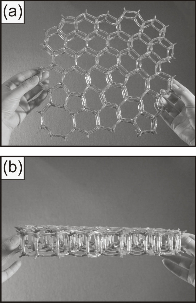
“This is the first time we have been able to directly observe which characteristic elements the structure possesses and which patterns occur in it,” says Markus Heyde. According to the observations, silicon and oxygen atoms take their turns in the individual silica layers and form a network of rings that lie next to each other like soap bubbles floating on water, and also assume sizes which differ almost as much – starting with rectangular rings with only four atoms through to those with nine or more atoms. Hexagonal rings are the most frequent, and the rings become all the rarer the further the number of their atoms deviates from six.
It had so far not been possible to check the structure proposed by William Zachariasen, as X-ray diffraction, the method of choice to determine the structure of materials, cannot be used in glasses and in amorphous materials in general – at least, not for determining the precise positions of the atoms. The Berlin-based researchers succeeded in doing just this with a trick; however, they designed a two-dimensional model of a glass. In an ultrahigh vacuum chamber they produced just two atomic layers of silica on a substrate of the precious metal ruthenium, which they had earlier coated with an oxygen layer.
The completely planar structure allows the scientists to look at the structure
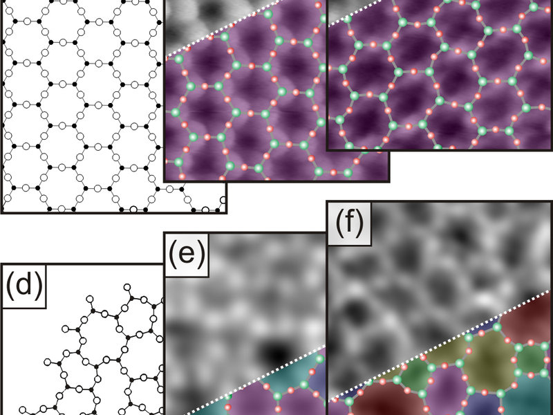
Late confirmation of a proposed structure: William Zachariasen already published his idea on how the atoms are arranged in a two-dimensional crystalline and amorphous network 80 years ago (a,d). Measurements with a scanning tunnelling microscope now confirm his suggestion (b,c and e,f). Depending on the contrast chosen, the silicon atoms (b,e) or oxygen atoms (c,f) can be seen in the Figures, which show a section measuring 3.5 by 2.4 nanometres. Atomic structures and ring sizes are marked in colour in the lower part of the images.
“Depending on how we change the temperature during the sample preparation, and how much silicon and oxygen we release in the vacuum, we obtain an amorphous or a crystalline structure, or even a mixture of both,” explains Leonid Lichtenstein, who investigated the different structures in his doctoral thesis. This allowed the researchers to produce silica surfaces which are so smooth that even the glass mirrors of the best telescopes in the world, which are polished to an extremely high level of precision, would look like hilly the Rocky Mountains by comparison.
“The structure of the two-dimensional glass provides us with important information about the structure of a three-dimensional glass,” says Markus Heyde. This is primarily due to the fact that the completely planar glass film allows researchers to view its very own structure for the first time. In planar surfaces the positions of the individual atoms can be determined, even if the structure is amorphous.
In a preliminary study, the scientists scanned amorphous silica with a scanning tunnelling microscope, which tells them where the oxygen atoms are located. This already revealed the irregular meshes of the network which William Zachariasen proposed as the structure of glass. In two further studies, the researchers also scanned the surfaces of their samples with a non-contact atomic force microscope which can also detect the silicon atoms. They thus obtained an accurate image of all atomic positions in the two-dimensional glass.
Knowing the glass structure helps to develop catalysts
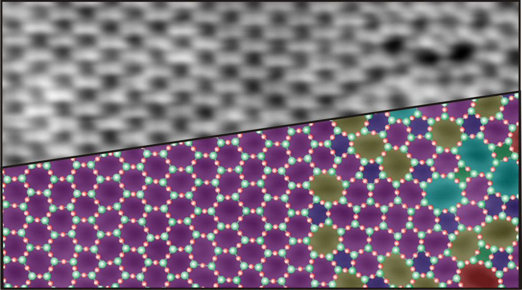
The scientists also investigated the transition between an amorphous and a crystalline silica film. “We determined that, apart from the hexagons, it is mainly pentagonal and heptagonal shapes that occur at the boundary initially – i.e. the most similar rings,” says Markus Heyde. The further they moved their microscope’s gaze from the crystalline to the amorphous region, the more the ring sizes deviated from the crystalline hexagonal structure.
The order disintegrates: During the transition from a crystalline to an amorphous silica structure, rings with five and seven atoms appear first, elements with a larger deviation from the hexagonal rings of the crystalline structure can be found only deeper in the disordered region.
Now that the researchers have a crystal-clear view of each individual atom in an amorphous silica film, they want to investigate how the different structural elements behave when foreign atoms or molecules end up on the glass surface. Do they attach preferentially to rings of a specific size? “We are interested in this question because such absorption processes are important for heterogeneous catalysis,” explains Hans-Joachim Freund, director at the Fritz Haber Institute.
Contacts and sources:
Dr. Markus Heyde
