


| Story Views | |
| Now: | |
| Last Hour: | |
| Last 24 Hours: | |
| Total: | |
This Is Huge! IBM Breakthrough To Replace Silicon

For the first time, scientists precisely place and test more than ten thousand carbon nanotube devices in a single chip using mainstream manufacturing processes
Novel processing method helps pave the way for carbon technology as a viable alternative to silicon in future computing
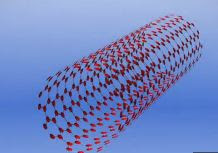
Carbon Nanotube
Aided by rapid innovation over four decades, silicon microprocessor technology has continually shrunk in size and improved in performance, thereby driving the information technology revolution. Silicon transistors, tiny switches that carry information on a chip, have been made smaller year after year, but they are approaching a point of physical limitation.
IBM SEM image of carbon nanotube field-effect transistor (CNTFET) arrays with a pitch of 300 nm. Source and drain contacts for the devices in the array are connected by metal leads and pads for electrical testing in a semi-automated probe station.

Carbon nanotubes represent a new class of semiconductor materials whose electrical properties are more attractive than silicon, particularly for building nanoscale transistor devices that are a few tens of atoms across. Electrons in carbon transistors can move easier than in silicon-based devices allowing for quicker transport of data. The nanotubes are also ideally shaped for transistors at the atomic scale, an advantage over silicon. These qualities are among the reasons to replace the traditional silicon transistor with carbon – and coupled with new chip design architectures – will allow computing innovation on a miniature scale for the future.
The approach developed at IBM labs paves the way for circuit fabrication with large numbers of carbon nanotube transistors at predetermined substrate positions. The ability to isolate semiconducting nanotubes and place a high density of carbon devices on a wafer is crucial to assess their suitability for a technology – eventually more than one billion transistors will be needed for future integration into commercial chips. Until now, scientists have been able to place at most a few hundred carbon nanotube devices at a time, not nearly enough to address key issues for commercial applications.
“Carbon nanotubes, borne out of chemistry, have largely been laboratory curiosities as far as microelectronic applications are concerned. We are attempting the first steps towards a technology by fabricating carbon nanotube transistors within a conventional wafer fabrication infrastructure,” said Supratik Guha, Director of Physical Sciences at IBM Research. “The motivation to work on carbon nanotube transistors is that at extremely small nanoscale dimensions, they outperform transistors made from any other material. However, there are challenges to address such as ultra high purity of the carbon nanotubes and deliberate placement at the nanoscale. We have been making significant strides in both.” 
Credit: IBM
Originally studied for the physics that arises from their atomic dimensions and shapes, carbon nanotubes are being explored by scientists worldwide in applications that span integrated circuits, energy storage and conversion, biomedical sensing and DNA sequencing.
This achievement was published today in the peer-reviewed journal Nature Nanotechnology.
The Road to Carbon
Carbon, a readily available basic element from which crystals as hard as diamonds and as soft as the “lead” in a pencil are made, has wide-ranging IT applications.

Credit: IBM
Carbon nanotubes are single atomic sheets of carbon rolled up into a tube. The carbon nanotube forms the core of a transistor device that will work in a fashion similar to the current silicon transistor, but will be better performing. They could be used to replace the transistors in chips that power our data-crunching servers, high performing computers and ultra fast smart phones.
Earlier this year, IBM researchers demonstrated carbon nanotube transistors can operate as excellent switches at molecular dimensions of less than ten nanometers – the equivalent to 10,000 times thinner than a strand of human hair and less than half the size of the leading silicon technology. Comprehensive modeling of the electronic circuits suggests that about a five to ten times improvement in performance compared to silicon circuits is possible.
There are practical challenges for carbon nanotubes to become a commercial technology notably, as mentioned earlier, due to the purity and placement of the devices. Carbon nanotubes naturally come as a mix of metallic and semiconducting species and need to be placed perfectly on the wafer surface to make electronic circuits. For device operation, only the semiconducting kind of tubes is useful which requires essentially complete removal of the metallic ones to prevent errors in circuits. Also, for large scale integration to happen, it is critical to be able to control the alignment and the location of carbon nanotube devices on a substrate.

Credit: IBM
The process starts with carbon nanotubes mixed with a surfactant, a kind of soap that makes them soluble in water. A substrate is comprised of two oxides with trenches made of chemically-modified hafnium oxide (HfO2) and the rest of silicon oxide (SiO2). The substrate gets immersed in the carbon nanotube solution and the nanotubes attach via a chemical bond to the HfO2 regions while the rest of the surface remains clean.

Credit: IBM
Furthermore, rapid testing of thousands of devices is possible using high volume characterization tools due to compatibility to standard commercial processes.
As this new placement technique can be readily implemented, involving common chemicals and existing semiconductor fabrication, it will allow the industry to work with carbon nanotubes at a greater scale and deliver further innovation for carbon electronics.
For more information, please visit www.research.ibm.com.
5 Crazy Conspiracy Theories About Hurricane Sandy
UFO over Hurricane Sandy Viewed from Space Station, Oct 2012.
UFO Emerges From Volcano And Cloaks Itself, Video
First Direct Detection Sheds Light On Dark Galaxies
The Altar At the Center Of The Milky Way
Demon Face In Space, Just In Time For Halloween
Protoplanet Vesta: Forever Young?
Unprecedented View Of 100 Galaxies In Our Local Universe
Green Tea Found To Reduce Rate Of Some GI Cancers
How Silver Can Turn Your Skin Blue
Special Mouthwash Could Swish Away Tooth Decay
Benghazi Timeline September 11-October 30
This Is Huge! IBM Breakthrough To Replace Silicon
First Ever Family Tree For All Living Birds Reveals Evolution And Diversification
