


| Story Views | |
| Now: | |
| Last Hour: | |
| Last 24 Hours: | |
| Total: | |
High vertical yield InP nanowire growth on Si(111) using a thin buffer layer
Thursday, October 24, 2013 8:45
% of readers think this story is Fact. Add your two cents.

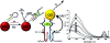
We demonstrate the growth of InP nanowires on Si(111) using a thin InP buffer layer. The buffer layer is grown using a two-step procedure. The initial layer formation is ensured by using a very low growth temperature. An extremely high V/III ratio is necessary to prevent In droplet formation at this low temperature. The second layer is grown on the initial layer at a higher temperature and we find that post-growth annealing of the buffer layer does not improve its crystal quality significantly. It is found that the layers inherently have the (111)B polarity. Nanowires grown on this buffer layer have the same morphology and optical properties as nanowires grown on InP (111)B substrates. The vertical yield of the nanowires grown on the buffer layer is over 97% and we also find that crystal defects in the buffer layer do not affect the morphology, vertical yield or optical properties of the nanowires significantly.
H A Fonseka, H H Tan, J Wong-Leung, J H Kang, P Parkinson and C Jagadish
Source: http://nanochemistry.blogspot.com/2013/10/high-vertical-yield-inp-nanowire-growth.html
