
| Online: | |
| Visits: | |
| Stories: |

| Story Views | |
| Now: | |
| Last Hour: | |
| Last 24 Hours: | |
| Total: | |
Towards A Sensitive Skin for Robots, Bridges, Aircraft and More with Printable Sensors
Covering a robot — or an airplane or a bridge — with sensors will require a technology that is both flexible and cost-effective to manufacture in bulk. A team of researchers at MIT’s Computer Science and Artificial Intelligence Laboratory thinks that 3-D printing could be the answer.
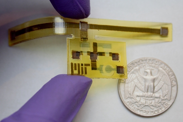
In an attempt to demonstrate the feasibility of flexible, printable electronics that combine sensors and processing circuitry and can act on their environments, the researchers have designed and built a device that responds to mechanical stresses by changing the color of a spot on its surface.
The device was inspired by the golden tortoise beetle, or “goldbug,” an insect whose exterior usually appears golden but turns reddish orange if the insect is poked or prodded — that is, mechanically stressed.
The researchers present their new design in the latest issue of the journal Advanced Materials Technologies. Sundaram is the first author on the paper, and the senior authors are Sundaram’s advisor, Wojciech Matusik, an associate professor of EECS; and Marc Baldo, a professor of EECS and director of the Research Laboratory of Electronics. Joining them on the paper are Pitchaya Sitthi-Amorn, a former postdoc in Matusik’s lab; Ziwen Jiang, an undergraduate EECS student; and David Kim, a technical assistant in Matusik’s Computational Fabrication Group.

Bottom up
Printable electronics, in which flexible circuitry is deposited on some type of plastic substrate, has been a major area of research for decades. But Sundaram says that the ability to print the substrate itself greatly increases the range of devices the technique can yield.
For one thing, the choice of substrate limits the types of materials that can be deposited on top of it. Because a printed substrate could consist of many materials, interlocked in intricate but regular patterns, it broadens the range of functional materials that printable electronics can use.
Printed substrates also open the possibility of devices that, although printed as flat sheets, can fold themselves up into more complex, three-dimensional shapes. Printable robots that spontaneously self-assemble when heated, for instance, are a topic of ongoing research at the CSAIL Distributed Robotics Laboratory, led by Daniela Rus, the Andrew and Erna Viterbi Professor of Electrical Engineering and Computer Science at MIT.
“We believe that only if you’re able to print the underlying substrate can you begin to think about printing a more complex shape,” Sundaram says.
Selective signaling
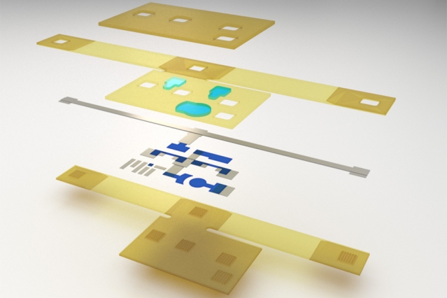
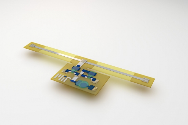
The MIT researchers’ new device is approximately T-shaped, but with a wide, squat base and an elongated crossbar. The crossbar is made from an elastic plastic, with a strip of silver running its length; in the researchers’ experiments, electrodes were connected to the crossbar’s ends. The base of the T is made from a more rigid plastic. It includes two printed transistors and what the researchers call a “pixel,” a circle of semiconducting polymer whose color changes when the crossbars stretch, modifying the electrical resistance of the silver strip.
The components that make up the printable device.
Image: Subramanian Sundaram
In fact, the transistors and the pixel are made from the same material; the transistors also change color slightly when the crossbars stretch. The effect is more dramatic in the pixel, however, because the transistors amplify the electrical signal from the crossbar. Demonstrating working transistors was essential, Sundaram says, because large, dense sensor arrays require some capacity for onboard signal processing.
Sundaram added a copper-and-ceramic heater, which was necessary to deposit the semiconducting plastic: The plastic is suspended in a fluid that’s sprayed onto the device surface, and the heater evaporates the fluid, leaving behind a layer of plastic only 200 nanometers thick.
Fluid boundaries
A transistor consists of semiconductor channel on top of which sits a “gate,” a metal wire that, when charged, generates an electric field that switches the semiconductor between its electrically conductive and nonconductive states. In a standard transistor, there’s an insulator between the gate and the semiconductor, to prevent the gate current from leaking into the semiconductor channel.
Researchers have designed and built a device that responds to mechanical stresses by changing the color of a spot on its surface.
Image: Subramanian Sundaram
“I am very impressed with both the concept and the realization of the system,” says Hagen Klauk, who leads the Organic Electronic Research Group at the Max Planck Institute for Solid State Research, in Stuttgart, Germany. “The approach of printing an entire optoelectronic system — including the substrate and all the components — by depositing all the materials, including solids and liquids, by 3-D printing is certainly novel, interesting, and useful, and the demonstration of the functional system confirms that the approach is also doable. By fabricating the substrate on the fly, the approach is particularly useful for improvised manufacturing environments where dedicated substrate materials may not be available.”
Source: http://www.ineffableisland.com/2017/03/towards-sensitive-skin-for-robots.html


